Semiconductor solutions
In the semiconductor manufacturing process, wafers are following a trend toward ever thinner thicknesses. Nikon s outstanding proprietary technology makes optimal solutions for these “no-error” market.
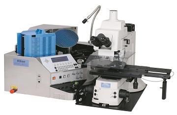
NWL200: Nikon Wafer Loader 200
- Fully secured wafer loader to our L200N microscopes for full manual or automated inspection.
- Incl: wafer alignment, cross-slot-detection, mark detection (notch, flat or double flat), cassette programs, sample programs, good/not-good put back, 6 & 8 inch…
- Option: Macro inspection, Macro image capturing, IR, …
NWL200 + L200N
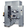
Automated systems:
- 6,8,12 inch loader with L200 or L300 microscope
- Extra KLARF compare
- Extra wobler/macro
- 1 or 2 port loader
- Clossed or open system
- 6,8,12 inch loader with NEXIV system
- Same extra options as microscope setup
- NEXIV (VMZ-S range) for metrology purposes
- NEXIV (VMZ-K range) for metrology and topography purposes (confocal)
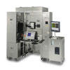
OST3200: OPTISTATION3200 (2 foup port)
Engineered to provide cost-effective support for 300mm wafers with a minimal footprint, the Optistation features an advanced micro/macro system in a compact, flexible design. The optical system offers brighter images, and observation techniques can be programmed for each objective magnification and each substrate layer to be inspected.
OST3100
OST3200
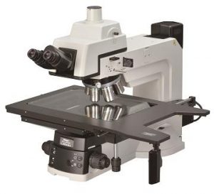
L300N